Iowa Industrial Moderated Newsgroup For Surplus Equipment > Manufacturing Equipment
> Press
> New
> 3090 / XC3090 / XC3090-100PQ160C / XC3090-100
3090 / XC3090 / XC3090-100PQ160C / XC3090-100
Now over 1,300 items in our Store!
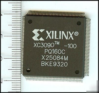
XC3090-100PQ160C Xilinx $9.99 each Please note: These parts are PULLS! The following spec sheet is provided by Xilinix and may cover several different versions and/or products. This listing is only for the item pictured and listed in the heading.
Part Number = XC3090-100PQ160C
Description = User Programmable Gate Array
Configurable Logic Blocks = 320
Logic Level Family = CMOS and T
V(OL)Max.(V)Lo Level Out.Volt. = 0.4
V(OH)Min.(V)Hi Level Out.Volt. = 3.86
Vsup(+) Nom.(V) Pos.Sup.Volt. = 5
Quiescent Current Max (CMOS) = 500u
Quiescent Current Max (TTL) = 10m
JEDEC Std 30 Outline Code = S-PQFP-G
Package Body Material = Plastic
• Complete line of five related Field Programmable
– XC3000, XC3000A, XC3000L, XC3100, XC3100A
• Ideal for a wide range of custom VLSI design tasks
– Replaces TTL, MSI, and other PLD logic
– Integrates complete sub-systems into a single package
– Avoids the NRE, time delay, and risk of conventional masked gate arrays
• High-performance CMOS static memory technology
– Guaranteed toggle rates of 70 to 325 MHz, logic delays from 9 to 2.2 ns
– System clock speeds over 80 MHz
– Low quiescent and active power consumption
– Compatible arrays ranging from 1,000 to 7,500 gate complexity
– Extensive register, combinatorial, and I/O capabilities
– High fan-out signal distribution, low-skew clock nets
– Internal 3-state bus capabilities
– TTL or CMOS input thresholds
– On-chip crystal oscillator amplifier
– Standard, off-the-shelf product availability
– 100% factory pre-tested devices
– Excellent reliability record
• Complete XACT Development System
– Schematic capture, automatic place and route
– Interactive design editor for design optimization
– Interfaces to popular design environments like Viewlogic, Cadence, Mentor Graphics, and others
The CMOS XC3000 Class of Logic Cell Array (LCA) families provide a group of high-performance, high-density, digital integrated circuits. Their regular, extendable, flexible, user-programmable array architecture is composed of a configuration program store plus three types of configurable elements: a perimeter of I/O Blocks (IOBs), a core array of Configurable Logic Bocks (CLBs) and resources for interconnection. The general structure of an LCA device is shown in Figure 1 on the next page. The XACT development system provides schematic capture and auto place-and-route for design entry. Logic and timing simulation, and in-circuit emulation are available as design verification alternatives. The design editor is used for interactive design optimization, and to compile the data pattern that represents the configuration program.
The LCA user logic functions and interconnections are determined by the configuration program data stored in internal static memory cells. The program can be loaded in any of several modes to accommodate various system requirements. The program data resides externally in an EEPROM, EPROM or ROM on the application circuit board, or on a floppy disk or hard disk. On-chip initialization logic provides for optional automatic loading of program data at power-up. The companion XC17XX Serial Configuration PROMs provide a very simple serial configuration program storage in a one-time programmable package.